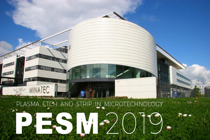
Askar Rezvanov, a production engineer of the MERI technological design department participated in PESM (Plasma Etch and Strip in Microtechnology) workshop that took place on May 21-22 in Grenoble, home of CEA-Leti - one of the world’s largest microelectronics research centers.
Every year PESM workshop gathers the researchers and microelectronic components manufacturers from around the world who reports on their results in developing etching processes used for semiconductor ICs manufacturing.
Askar Rezvanov presented two reports: “A Novel Volatile Film for Dielectric Plasma Damage Protection”, prepared together with colleagues from Imec and TEL and “The process of low-temperature etching of porous low-k dielectrics in C2F4Br2 plasma”, performed in collaboration with colleagues from the Institute of Physics and Technology, RAS and MIREA - Russian Technological University.
The program of the workshop included 4 sections:
- Advanced Etching & Stripping for CMOS (included report on Plasma etching for FinFet, STI and Low-k dielectrics);
- Etching and Stripping for more than Moore applications (reports on Plasma etching and stripping for MEMS, bio MEMS, imagers, photonics and 3D IC);
- Plasma fundamentals (included reports on New plasma sources and Advanced plasma diagnostics);
- New Processes/New materials (this section was devoted to Atomic Layer Etching, Plasma etching and stripping for III-V materials (HEMT, CMOS, etc.) and for memories (MRAM, OXRAM, etc.).
Most of the reports were prepared by young scientists. The organizers and participants of PESM estimated the high level of reports, and also expressed a desire to expand the range of discussion topics in future.
Note:
PESM – Plasma Etch and Strip in Microtechnology – an international workshop devoted to plasma etch and strip processes for micro, nano and bio- technologies. The Forum is aimed at scientists and engineers of nano- and microelectronics. The topics usually include both fundamental and applied research as well as issues related to the progressive downscaling of device dimensions.
More information:
http://pesm2019.insight-outside.fr/en/topics/1