

Cryptography developed at MERI for civilian drones
Global Navigation Satellite System (GLONASS) and the Element Group of Companies (Element) have introduced an identifier for civilian air drones…
15.07.2026
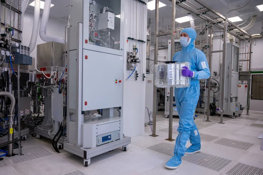
Molecular Electronics Research Institute (MERI) and Scientific Research Institute of Precision Mechanics have completed the development and packaging of the first cluster systems in Russia for plasma-enhanced chemical vapor deposition and plasma etching processes. The installations will allow the production of IC according to the 65 nm topological standards on 200 mm and 300 mm wafers. Russian organizations have entered the top five companies in the world with expertise in the development and production of this class of technological equipment. The installations were created with the support of the Ministry of Industry and Trade of Russia.
The main contractor of the project was MERI, which provided the construction of clean production facilities, the installation and connection of prototype equipment in clean rooms, the development of technological processes and the testing of equipment. The main co-contractor was Scientific Research Institute of Precision Mechanics, which specialists developed the equipment itself and participated in the testing.
«The creation of the first Russian cluster systems for plasma-enhanced chemical vapor deposition and plasma etching processes is an important practical achievement. 65 nm level installations on 300 mm wafers will also meet the prospective needs of domestic microelectronics. A particular value is represented by the modularity of the platform: it allows processes to be practiced on existing equipment and serves as a basis for transitioning to more refined technological processes. This project demonstrates that the cooperation of Russian scientific institutes and industry is capable of solving the most complex technological tasks», noted Vasily Shpak, the Deputy Minister of Industry and Trade.
In global practice cluster-type, equipment is used as the standard for chip production, as it allows combining from 2 to 8 technological units with a common loading system. This provides the ability to consecutively carry out a series of technological processes without unloading the plates into the room's atmospheric environment. The modular structure allows for flexible configuration of the equipment depending on the needs and capacity of production. All these factors affect the reduction of production costs and the improvement of chip quality.
Today technological processes with topological norms of 28-90 nm in the global market provide the most mass production of microchips for the automotive and aerospace industries as well as automation and control systems.
The equipment is designed to work with wafers with a diameter of 200 and 300 mm. This provides the opportunity to apply setups in both existing and planned productions with technological standards implemented on 200 mm wafers as well as to ensure timely preparation for the transition to working with 300 mm wafers. When using the equipment configuration for 200 mm wafers, it is possible to use with the design standards — 90, 130, 180, 250 nm.
In the future the basic technological processes of deposition and etching of dielectric layers developed and certified within the project will serve as a basis for their adaptation to existing technological processes and for the development of advanced ones, including 28 nm.
«Entering the global top of holders of cluster system technology for microelectronics is both a colossal achievement and a serious responsibility towards Russian developers. The creation of Russian cluster systems for plasma-enhanced chemical vapor deposition and plasma etching processes has become a key stage on the way to the technological independence of domestic microelectronics. We have laid the foundation for further development», said Alexander Kravtsov, CEO of MERI.
«The clusters’ development for plasma-enhanced chemical vapor deposition and plasma etching processes installations for processing 300 mm silicon wafers opens new prospects for bringing the Russian microelectronics industry to a new technological level. The equipment development for technologies with a design rule of up to 65 nm is an important step in the Russia's electronics industry development, demonstrating a high level of expertise and the readiness to provide Russian companies with their own equipment that is not inferior to foreign counterparts», said Mikhail Biryukov, CEO of Scientific Research Institute of Precision Mechanics.
Company Information:
Element Group of Companies (MOEX:ELMT) is a leader in the production of domestic electronic components. The Group's products are used in key sectors of the Russian economy, including healthcare, energy, transport, oil and gas industry, aircraft and shipbuilding, as well as the space industry. The Group includes more than 30 design centers and production facilities. The Group manufactures over 3,000 product types. In May 2024, Element conducted an IPO. In January 2026, AFK Sistema, which owned 37.6% of the shares, completely exited the shareholders of Element, selling its stake to Sberbank.
JSC «Scientific Research Institute of Precision Mechanics», part of the Element Group of Companies, MOEX: ELMT) is a leading developer and manufacturer of a wide range of industrial and research technological equipment for the microelectronics industry. The institute was founded in 1962. It is engaged in the creation of plasma chemical etching, vapor phase deposition, physical deposition, epitaxial structure growth, and gas-thermal processing installations, as well as cluster complexes based on them for processing wafers up to 300 mm in diameter. It is an active participant in Integrated Projects and State programs of the Ministry of Industry and Trade of the Russian Federation. It is included in the register of organizations operating in the field of the radio-electronic industry.
JSC «Research Institute of Molecular Electronics», part of the Element Group of Companies, MOEX: ELMT) is a leading research center conducting fundamental and applied research in the field of microelectronics, as well as the development and production of semiconductor products. It was founded in 1964. It carries out experimental design work under programs of the Ministry of Industry and Trade, the Ministry of Science and Higher Education, state corporations, and also conducts initiative work at its own expense. By the decree of the Government of the Russian Federation, it is designated as the organization responsible for implementing the priority area «Electronic Technologies». Resident of the special economic zone «Technopolis Moscow».
Global Navigation Satellite System (GLONASS) and the Element Group of Companies (Element) have introduced an identifier for civilian air drones…
On July 10, 2026, in Yekaterinburg, Molecular Electronics Research Institute (part of the Element Group of Companies, MOEX:ELMT) presented domestic…
The Saint Petersburg Electrotechnical University "LETI" held a roundtable discussion as part of the II International Forum on Microelectronics and…